PLI International
Laser Direct Imaging (Ldi) PCB
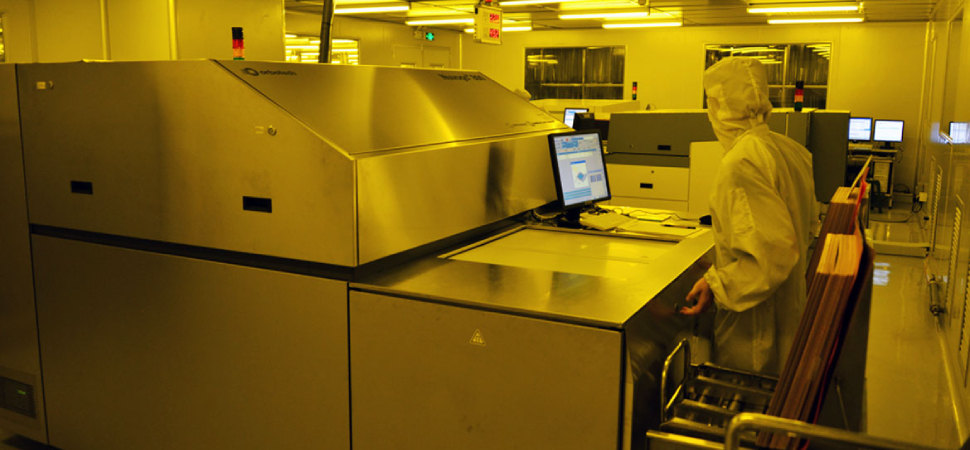
Laser Direct Imaging (LDI) for PCB (Printed Circuit Board) is a process used in electronics manufacturing to create fine traces and patterns on PCBs using a laser. This process replaces traditional photolithography methods that use a mask and UV light to create the desired pattern.

PLI International
Laser Direct Imaging (Ldi) PCB
LDI works by using a high-powered laser to directly expose the photoresist material on the PCB. The laser beam is guided by a computer-controlled system that follows the desired pattern for the PCB. The laser can create very fine features with high precision, making it ideal for producing PCBs with high-density components and small form factors.
One of the main advantages of LDI is that it eliminates the need for a physical mask, reducing the time and cost required for the mask-making process. It also enables faster prototyping and production of PCBs with shorter lead times. LDI also offers higher accuracy and resolution than traditional photolithography, resulting in a higher-quality product.
Another advantage of LDI is that it is a more environmentally friendly process compared to traditional photolithography. The LDI process does not use any harsh chemicals, reducing the environmental impact of the manufacturing process.
LDI is widely used in the electronics manufacturing industry, particularly in the production of high-density interconnect PCBs and flexible PCBs.
Flex Boards / HDI / Multi Layer Boards / Rigid Flex Boards
